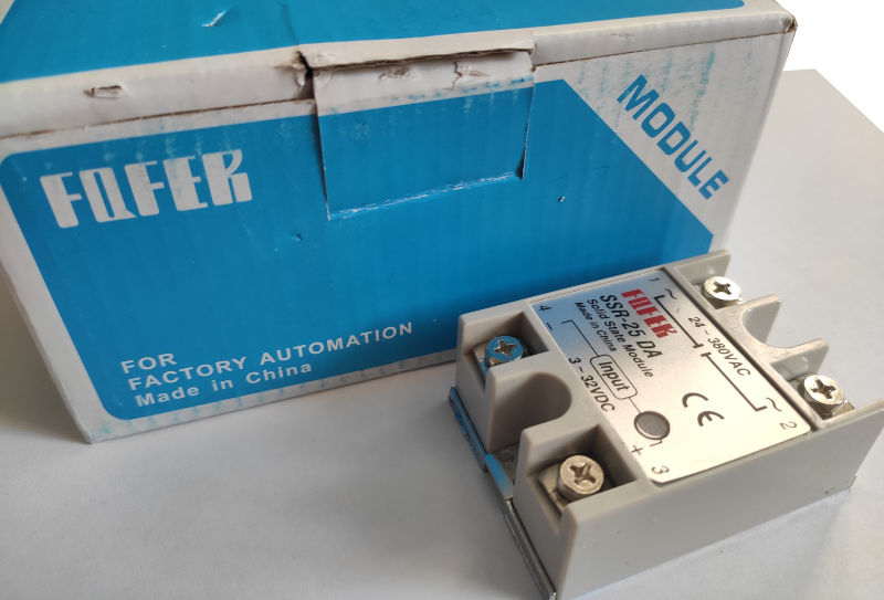
FQFER instead of FOTEK
On the Lunar New Year Eve, I won an Aliexpress scam lottery and, instead of the genuine FOTEK SSR-25 DA solid state relay (SSR) or even a fake FOTEK, which I actually expected, I received something called FQFER SSR-25 DA. The price was around 350 ₽ (3.5 USD) per unit, and 5 units came in a beatiful blue box suggesting that the SSRs were made in a kind of a factory that can afford ordering beautiful blue boxes for packaging their products.
Where I work, we use plenty of (probably fake) FOTEK SSR-25 DA. Surprisingly, they are fairly reliable and long-lasting, especially for currents up to around 10 A, which is more then enough for our typical small laboratory furnaces. We cracked open one of our dead FOTEK SSR-25 DA once, and it looked pretty much like in this guy’s video here:
However, I haven’t found anything detailed on, ahem, these particular FQFER on the Web, aside from unrelated scary stories about how the optocouplers in some fake “zero-crossing” SSRs were not actually zero-crossing, and some photos of the FQFER SSR-40 AA in one of the EEVblog posts. So I decided to tear one down and take a sneaky peek inside.
Teardown
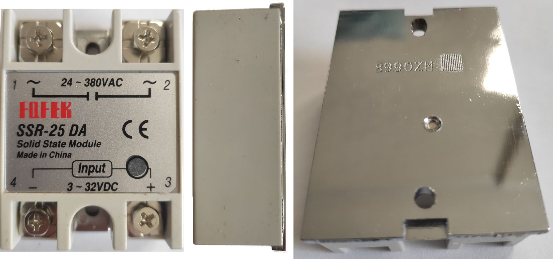
Here’s the top, side and bottom views of the relay. On the latter you see the threaded hole for screwing (don’t you worry, there will be a pun below) the triac to the base plate. There’s nothing especially interesting here aside from the font of the FQFER logo that intends to mimic the original FOTEK font. Cringey! Things like this give designers the creeps. This time, I’m glad I’m not a designer.
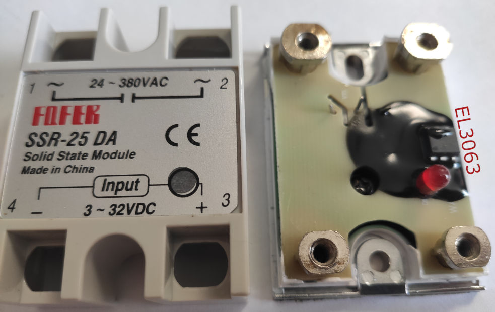
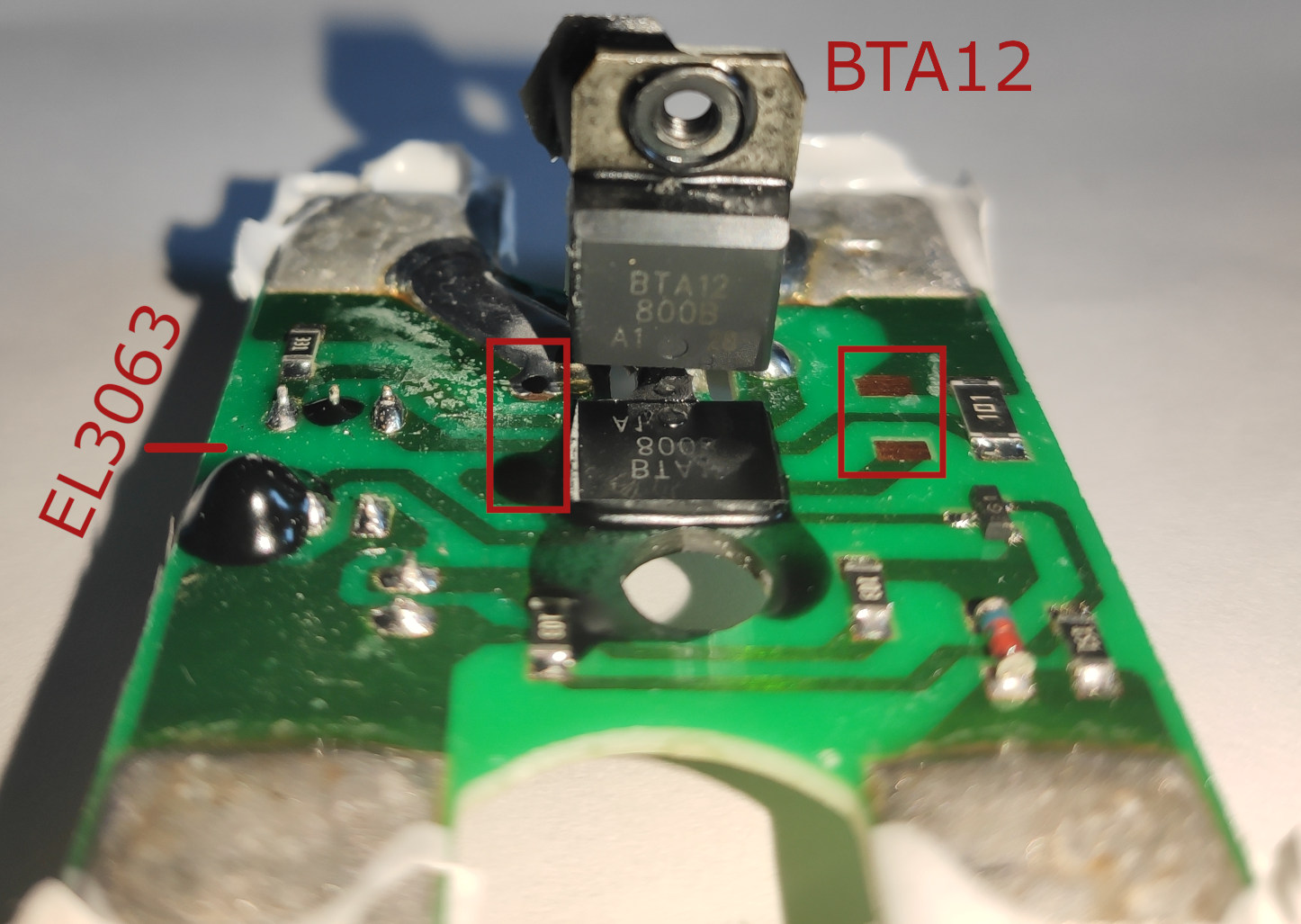
After unscrewing the terminals I was able to pry the plastic cover off the base plate with a scalpel. This was easier than I expected because the thing had been held together with a small amount of silicone sealant (whitish soft goo, which is barely seen around the PCB in the foto below). The black solid goo is some kind of (probably epoxy) resin. The only three through-hole components in this SSR are the triac, of which only the leads are seen so far, the LED, and the optocoupler. Luckily, it’s an EL 3063, a zero-crossing optocoupler. In this image as well as in the following ones the low-voltage (controlling) curcuitry is at the bottom, and the high-voltage parts - at the top.
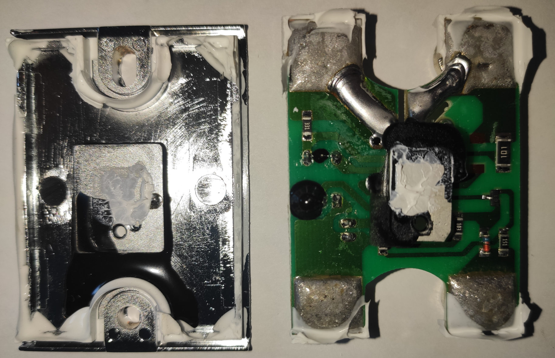
After unscrewing the triac and tapping its heatsink lightly with a hammer (via a screwdriver) to free the poor semiconductor from the oppression of the resin, I detached the triac with the PCB from the base plate.
The horror! The horror!
It is seen that some of the black resin that surrounds the triac somehow got under its heatsink, i.e., in-between the triac and the base plate. This prevents the contact between the triac and the plate, which no amount of heat conductive paste, located in the giant air gap between the two, could fix. It looks as if someone poured the resin before screwing the triac in place, or else made a very bad job of screwing. Screwed up, so to speak. Alas! Poor triac, destined to function effectively without external heatsink.
Aside from the horror, we see a bunch of SMD resistors, one SOT-23 NPN transistor marked G1, and one zener diode. I couldn’t determine which exactly transistor this G1 is, but it is probably something commonplace, like BC847B, or its pin-compatible comrade. There are no capacitors meaning there’s no RC snubber, making this device unsuitable for inductive loads (without external snubber, that is).
Below is the tilted view of the PCB with the triac detached. The triac is a BTA12-800B, capable of handling 12 A RMS current. Curiously, there are unsoldered pads on this PCB (marked with red rectangles in the photo) exactly where the snubber circuit might have been.
Circuitry
By tracing the wires and desoldering the zener (had to do this to determine its breakdown voltage) I came to the following schematics.
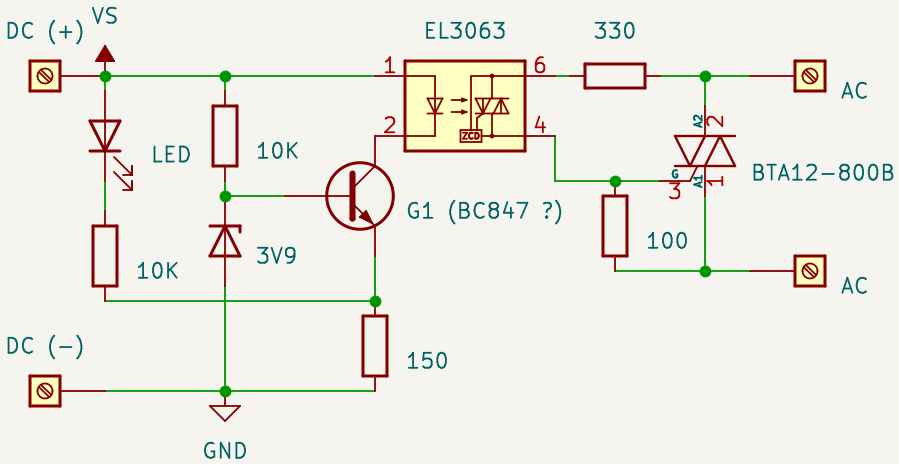
Input
The trigger current (input circuit) draws around 13.1 mA from the 12.1 V power supply that I used for the tests. Not bad. Interestingly, during the test, the zener’s reverse voltage was just 2.4-2.5 V due to the very low current through it. This voltage value is way below the reverse voltage that I determined at 30 mA current. This dirty trick with the zener’s nonlinear I-V characteristics is also good, as it limits further the current through the transistor. I didn’t check this experimentally, but quick calculations show that there should be enough current (>5 mA) to be able to turn the optocoupler on even at lower input voltages of 3-5 V. However, I wouldn’t recommend using higher voltages (24-32 V) to drive this SSR because more power will be dissipated in the transistor, which in its meager SOT-23 package with very limited power dissipation capability could quickly become very hot. For instance, at 32 V input voltage, even assuming 2.5 V zener voltage, I’ve got >0.25 W power dissipation in the transistor. This should be multiplied by several hundred K/W thermal resistance to get the temperature increase above ambient.
Output
Given the quality of these FQFER, let’s assume that we’re operating triacs in these SSR with no heatsink at all. So, we have, say, the ambient temperature of 25 °C. From the datasheet, we obtain 125 °C maximum junction temperature and 60 K/W junction-to-ambient thermal resistance of the TO220 package. This gives us 5/3 W maximum power. The maximum RMS current value corresponding to this power can be obtained either by using the plot from the BTA12 datasheet (Maximum power dissipation versus RMS on-state current) or by calculating with these Philips AN10384 recommendations, taking the static Rs and V0 characteristics from the datasheet. For our temperatures and thermal characteristics, both ways yield the same value of max RMS current. This value is almost exactly 2 A. Far cry from the 25 A rating, isn’t it?
Conclusions
Q: Is it a scam?
A: Definitely! If only because these SSR are labelled and sold as if they could be operated at 25 A. And I’m not even talking about the manufacturing quality.
Q: Are these SSR safe to use?
A: Well… kinda, given that the heatsink of the BTA12 triac is isolated (no mains on the base plate) and that there’s a zero-crossing optocoupler inside. That is, provided that (a) the individual electrical components meet their specifications and weren’t picked up from discarded defective semiconductor trash pile and (b) there will be no further manufacture-related surprises. And these SSR must not be used for switching high-power loads (see below).
Q: What is the recommended operating mode?
A: Try to keep the input voltage lower (5-12 V should be safe) and the output current well below the actual absolute maximum of about 2 A.
Q: Is there anything good about these SSR?
A: Well, the good news is, we don’t need those bulky external heatsinks anymore! With such maximal working currents and such assembling quality, they are simply not necessary. The other good thing is their repairability - there’s so little sealant and resin and they are so easy to remove that it’s highly likely that you’ll be able to replace a burned-off triac and even enhance the heat contact in the process. Speaking of heat contact, by the way, take a look at the back plate (this image). See how there are a few threads visible in the hole with the bolt holding the triac on the other side? In the properly made cheap SSR modules the bolt is more or less flush with the plate with no “extra” internal thread visible. This is how you can check your SSRs for the signs of improperly screwed triacs before putting the said SSRs into operation to prevent your device from being, well, screwed by the blasted triac.
UPDATE: I’ve got a pretty 50% cash return for these SSR on Aliexpress, which is also not bad.